- 您现在的位置:买卖IC网 > Sheet目录3855 > PIC18LF1230-I/ML (Microchip Technology)IC PIC MCU FLASH 2KX16 28QFN
PIC18F1230/1330
2009 Microchip Technology Inc.
DS39758D-page 111
13.0
TIMER1 MODULE
The Timer1 timer/counter module has the following
features:
16-bit timer/counter
(two 8-bit registers; TMR1H and TMR1L)
Readable and writable (both registers)
Internal or external clock select
Interrupt on overflow from FFFFh to 0000h
Status of system clock operation
Figure 13-1 is a simplified block diagram of the Timer1
module.
Register 13-1 details the Timer1 Control register. This
register controls the operating mode of the Timer1
module and contains the Timer1 Oscillator Enable bit
(T1OSCEN). Timer1 can be enabled or disabled by
setting or clearing control bit, TMR1ON (T1CON<0>).
The Timer1 oscillator can be used as a secondary clock
source in power-managed modes. When the T1RUN bit
is set, the Timer1 oscillator provides the system clock. If
the Fail-Safe Clock Monitor is enabled and the Timer1
oscillator fails while providing the system clock, polling
the T1RUN bit will indicate whether the clock is being
provided by the Timer1 oscillator or another source.
Timer1 can also be used to provide Real-Time Clock
(RTC) functionality to applications with only a minimal
addition of external components and code overhead.
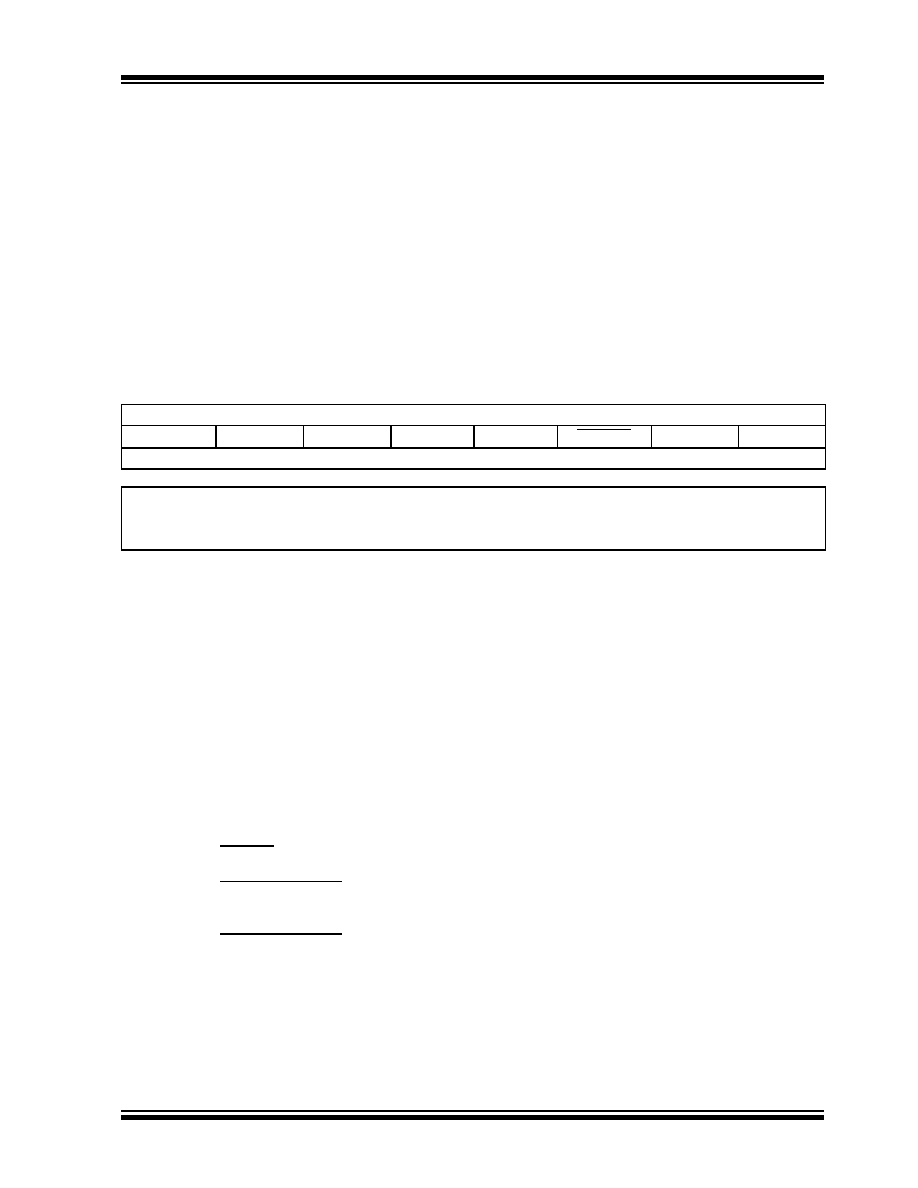
REGISTER 13-1:
T1CON: TIMER1 CONTROL REGISTER
R/W-0
R-0
R/W-0
RD16
T1RUN
T1CKPS1
T1CKPS0
T1OSCEN
T1SYNC
TMR1CS
TMR1ON
bit 7
bit 0
Legend:
R = Readable bit
W = Writable bit
U = Unimplemented bit, read as ‘0’
-n = Value at POR
‘1’ = Bit is set
‘0’ = Bit is cleared
x = Bit is unknown
bit 7
RD16:
16-Bit Read/Write Mode Enable bit
1
= Enables register read/write of Timer1 in one 16-bit operation
0
= Enables register read/write of Timer1 in two 8-bit operations
bit 6
T1RUN:
Timer1 System Clock Status bit
1
= Device clock is derived from Timer1 oscillator
0
= Device clock is derived from another source
bit 5-4
T1CKPS1:T1CKPS0:
Timer1 Input Clock Prescale Select bits
11
= 1:8 Prescale value
10
= 1:4 Prescale value
01
= 1:2 Prescale value
00
= 1:1 Prescale value
bit 3
T1OSCEN:
Timer1 Oscillator Enable bit
1
= Timer1 oscillator is enabled
0
= Timer1 oscillator is shut off
The oscillator inverter and feedback resistor are turned off to eliminate power drain.
bit 2
T1SYNC:
Timer1 External Clock Input Synchronization Select bit
When TMR1CS = 1:
1
= Do not synchronize external clock input
0
= Synchronize external clock input
When TMR1CS = 0:
This bit is ignored. Timer1 uses the internal clock when TMR1CS = 0.
bit 1
TMR1CS:
Timer1 Clock Source Select bit
1
= External clock from T1OSO/T1CKI (on the rising edge)(1)
0
= Internal clock (FOSC/4)
bit 0
TMR1ON:
Timer1 On bit
1
= Enables Timer1
0
= Stops Timer1
Note 1:
Placement of T1OSI and T1OSO/T1CKI depends on the value of the Configuration bit, T1OSCMX, of CONFIG3H.
发布紧急采购,3分钟左右您将得到回复。
相关PDF资料
PIC16LC711-04/SS
IC MCU OTP 1KX14 A/D 20SSOP
PIC18F65K22-I/MRRSL
MCU PIC 32K FLASH MEM XLP 64QFN
PIC16LF87-I/SS
IC MCU FLASH 4KX14 EEPROM 20SSOP
PIC16C62B-20/SS
IC MCU OTP 2KX14 PWM 28SSOP
PIC16LC711-04I/SO
IC MCU OTP 1KX14 A/D 18SOIC
PIC18F66J90-I/PT
IC PIC MCU FLASH 64KB 64-TQFP
ATMEGA32L-8AC
IC AVR MCU 32K LV 8MHZ COM44TQFP
DSPIC30F2012-30I/SP
IC DSPIC MCU/DSP 12K 28DIP
相关代理商/技术参数
PIC18LF1230-I/P
功能描述:8位微控制器 -MCU 4KB 256byt-RAM 16I/O RoHS:否 制造商:Silicon Labs 核心:8051 处理器系列:C8051F39x 数据总线宽度:8 bit 最大时钟频率:50 MHz 程序存储器大小:16 KB 数据 RAM 大小:1 KB 片上 ADC:Yes 工作电源电压:1.8 V to 3.6 V 工作温度范围:- 40 C to + 105 C 封装 / 箱体:QFN-20 安装风格:SMD/SMT
PIC18LF1230-I/SO
功能描述:8位微控制器 -MCU 4KB 256byt-RAM 16I/O RoHS:否 制造商:Silicon Labs 核心:8051 处理器系列:C8051F39x 数据总线宽度:8 bit 最大时钟频率:50 MHz 程序存储器大小:16 KB 数据 RAM 大小:1 KB 片上 ADC:Yes 工作电源电压:1.8 V to 3.6 V 工作温度范围:- 40 C to + 105 C 封装 / 箱体:QFN-20 安装风格:SMD/SMT
PIC18LF1230-I/SS
功能描述:8位微控制器 -MCU 4KBFlash 256byte-RAM 16 I/O 8-bit Family RoHS:否 制造商:Silicon Labs 核心:8051 处理器系列:C8051F39x 数据总线宽度:8 bit 最大时钟频率:50 MHz 程序存储器大小:16 KB 数据 RAM 大小:1 KB 片上 ADC:Yes 工作电源电压:1.8 V to 3.6 V 工作温度范围:- 40 C to + 105 C 封装 / 箱体:QFN-20 安装风格:SMD/SMT
PIC18LF1320-I/ML
功能描述:8位微控制器 -MCU 8KB 256 RAM 16I/O RoHS:否 制造商:Silicon Labs 核心:8051 处理器系列:C8051F39x 数据总线宽度:8 bit 最大时钟频率:50 MHz 程序存储器大小:16 KB 数据 RAM 大小:1 KB 片上 ADC:Yes 工作电源电压:1.8 V to 3.6 V 工作温度范围:- 40 C to + 105 C 封装 / 箱体:QFN-20 安装风格:SMD/SMT
PIC18LF1320-I/P
功能描述:8位微控制器 -MCU 8KB 256 RAM 16I/O RoHS:否 制造商:Silicon Labs 核心:8051 处理器系列:C8051F39x 数据总线宽度:8 bit 最大时钟频率:50 MHz 程序存储器大小:16 KB 数据 RAM 大小:1 KB 片上 ADC:Yes 工作电源电压:1.8 V to 3.6 V 工作温度范围:- 40 C to + 105 C 封装 / 箱体:QFN-20 安装风格:SMD/SMT
PIC18LF1320-I/SO
功能描述:8位微控制器 -MCU 8KB 256 RAM 16I/O RoHS:否 制造商:Silicon Labs 核心:8051 处理器系列:C8051F39x 数据总线宽度:8 bit 最大时钟频率:50 MHz 程序存储器大小:16 KB 数据 RAM 大小:1 KB 片上 ADC:Yes 工作电源电压:1.8 V to 3.6 V 工作温度范围:- 40 C to + 105 C 封装 / 箱体:QFN-20 安装风格:SMD/SMT
PIC18LF1320-I/SOG
功能描述:8位微控制器 -MCU 8kBF 256RM 16I/O Lead Free Package RoHS:否 制造商:Silicon Labs 核心:8051 处理器系列:C8051F39x 数据总线宽度:8 bit 最大时钟频率:50 MHz 程序存储器大小:16 KB 数据 RAM 大小:1 KB 片上 ADC:Yes 工作电源电压:1.8 V to 3.6 V 工作温度范围:- 40 C to + 105 C 封装 / 箱体:QFN-20 安装风格:SMD/SMT
PIC18LF1320-I/SS
功能描述:8位微控制器 -MCU 8KB 256 RAM 16I/O RoHS:否 制造商:Silicon Labs 核心:8051 处理器系列:C8051F39x 数据总线宽度:8 bit 最大时钟频率:50 MHz 程序存储器大小:16 KB 数据 RAM 大小:1 KB 片上 ADC:Yes 工作电源电压:1.8 V to 3.6 V 工作温度范围:- 40 C to + 105 C 封装 / 箱体:QFN-20 安装风格:SMD/SMT